Ordering to Start for | ||||||||||||||||||||
NSR-SF100 | ||||||||||||||||||||
The New i-line Stepper Realizes Highly Accurate Mix and Match with
Scanners and High Throughput. | ||||||||||||||||||||
|
| ||||||||||||||||||||
| 1999-11-29 | ||||||||||||||||||||
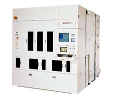 November 29, 1999 -- To create the most effective system for
non-critical layers of next-generation DRAMs and MPUs, Nikon
Corporation (YOSHIDA, Shoichiro, President) developed a new i-line
stepper, "NSR-SF100", and will start receiving orders for
the new system in January 2000. November 29, 1999 -- To create the most effective system for
non-critical layers of next-generation DRAMs and MPUs, Nikon
Corporation (YOSHIDA, Shoichiro, President) developed a new i-line
stepper, "NSR-SF100", and will start receiving orders for
the new system in January 2000. The NSR-SF100 is designed to realize superior cost performance in a mix and match strategy with Nikon KrF excimer laser scanners, which are now the main systems in state-of-the-art fab lines. The NSR-SF100 achieves a high resolution of 0.4 um or smaller and a 1 / 4 reduction ratio on an exposure field of 25 x 33 mm-the largest in the industry. The new i(I)-line stepper also boasts a high throughput of 120 or more wafers/hour for 200 mm wafers. In addition, the new system is compliant with full-scale 300 mm wafer fab lines, which are expected to be built in 2001. Sales Overview (Overview of Marketing Plan)
Development BackgroundBecause the density of VSLI increases constantly, as soon as we started the mass production of 128 Mb DRAMs, we were already moving toward the volume production of 256 Mb devices.A leader in this trend, Nikon unveiled the world's first KrF excimer laser scanner, the NSR-S201A, in April 1995. And currently, with the industry accelerating from 0.18 um to 0.15 um applications, we are marketing the KrF excimer laser scanners NSR-S204B and NSR-S203B, which meet the demands of the tighter design rules and have thus become the preferred systems on the most advanced fab line. In our standard "mix and match" approach, Nikon systems that are used for non-critical layers can perform up to the critical layers in the i-line range with a 0.35 um or better resolution. These systems include the i-line stepper NSR-2205i14E, with a 22x22 mm exposure field and a 1/5 reduction ratio, and the i-line scanner NSR-S103B, with a 25x33 mm exposure field and a 1/4 reduction ratio. The NSR-SF100 we are announcing today is a new i-line stepper for non-critical layers. The system was developed to work in a mix and match with KrF excimer laser scanners in leading-edge semiconductor production lines. The NSR-SF100 is optimized for exposing non-critical layers, which comprise about half of the total (20 or so) layers in a chip. In addition to sharing the same reduction ratio and exposure field size as those of the KrF excimer laser scanner, the NSR-SF100 attains the resolution and high throughput to create the requisite total balance and superior cost performance for the mix and match formation. It is a combination that will contribute to improving productivity and reducing the total investment cost of production lines. Main Features
Main Specifications
Colour of photographs appearing in this www site may differ from the originals. Specifications and equipment are subject to change without any notice or obligation on the part of the manufacturer. Nov. 1999 |